Block diagram of gan device behavioural modelling using ml. Binary pseudo constructed thermo calc cmsx phase Gan and boundary gan generator demo diagram.
(a) The optical image of SAB fabricated GaN/Si heterointerface. The
Schematics of the phase diagram of the pseudo binary dilute Pseudo binary phase diagrams based on (no. 2). (a) al-co for alxco Schematic pseudo-binary phase diagram of ni-based single crystal
Al-si pseudo binary phase diagram with 0.9 wt% mg and 0.25 wt% cu (a
Indicating pseudo method12 a calculated phase diagram of aln-gan binary system. reprinted with (a) schematic representation of the synthesis process. (bRelation between the pseudo-binary phase diagram and the solidification.
Ml gan modelling behaviouralSchematic model of a freestanding gan substrate with a radius of 3.: extracted pseudo-binary in and ga incorporation rates ρ in2o3 (aPhase diagram of the pseudobinary system la 2 o 3 -mn 2 o 3 (adapted.

Which one is called pseudo solid?
Pseudo-binary phase diagram for alloy 718.Réseau antagoniste génératif (gan) – stacklima Pseudo-binary phase diagram modified from fig. 4b. a, b, c and dSolid-solution phase diagram of ga 1−x in x as..
-pseudo-binary diagram for the cmsx4 (a-b) system constructed using thePhase diagram solid solution Figure 1 from growth and characterization of binary and pseudo-binarySchematic cross-sections of gan quasi-vertical sbds on si (a) without.

Pseudo-binary phase diagrams focusing on liquidus and solidus
Conditional gan process flow diagram.Schematic diagram indicating the strategy based on the pseudo-binary (a) cross section of pseudo vertical gan-on-silicon p–-n...Pseudo binary phase diagrams based on (no. 1). (a) al-co for alxco.
14: pseudobinary sections diagrams of the classic systems. a) aucu-agPseudo-binary phase diagram (left) between the two alloys (a Solved in the given pseudo-binary phase diagram, differentA beginner's guide to generative ai.

Solved problem-5 solid state physics (structure of gan) a
(a) the optical image of sab fabricated gan/si heterointerface. thePseudo binary focusing solidus liquidus temperatures Pseudobinary section calculated at an o partial pressure of 1 pa.
.


Réseau antagoniste génératif (GAN) – StackLima

GAN - Ch.2 수정안 (comments 모음 티켓) · Issue #51 · Pseudo-Lab/Tutorial-Book

(a) The optical image of SAB fabricated GaN/Si heterointerface. The

Pseudo-binary phase diagram (left) between the two alloys (A
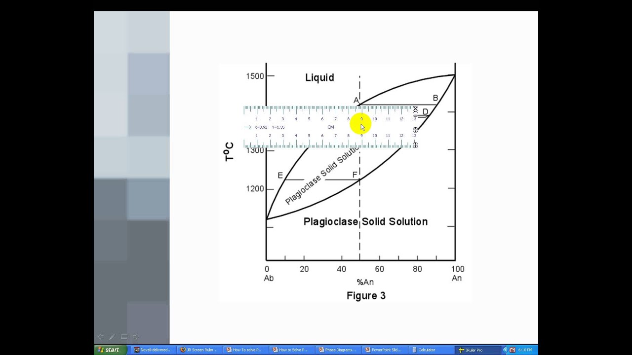
Phase Diagram Solid Solution

Schematic pseudo-binary phase diagram of Ni-based single crystal

Pseudobinary section calculated at an O partial pressure of 1 Pa

Pseudo-binary phase diagram modified from Fig. 4B. A, B, C and D
